Bare Die Introduction
With the advent of multichip modules (MCMs) and system in a package (SiP) applications,
customer demand for known good die (KGD) has increased offer the KGD for the discrete
products
KGD: Know Good Die
defined by JESD49A
Quality conformance to the applicable method 2010 of MIL-STD-883; methods 2072 and 2073 of
MIL-STD-750.
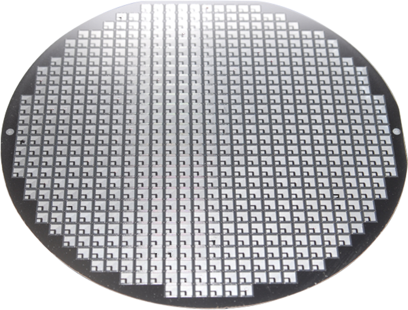
Package
- Whole wafers
- Waffle Pack
- Wafer on film frame
- In vials
- Tape on Reel